


ET Board
ET Board
High selective anisotropic etching
ET process by SCHMID is a new process which is capable to process line & space down to 2µm with an embedded trace technology based on the next generation of production tools. Major process steps to reach the objective were newly developed. The creation of the trace into a nonfiber material like ABF or Polyimide is done by a Plasma-etching process. The newly developed system combines a high selective anisotropic etching with no dust produced from the silica particles being present in the material.

Technical Data
All equipments developed for this process are capable to handle panel size of 610 x 610mm and minimal thickness of 25µm on a touch free mode.
Tools related to the ET process:
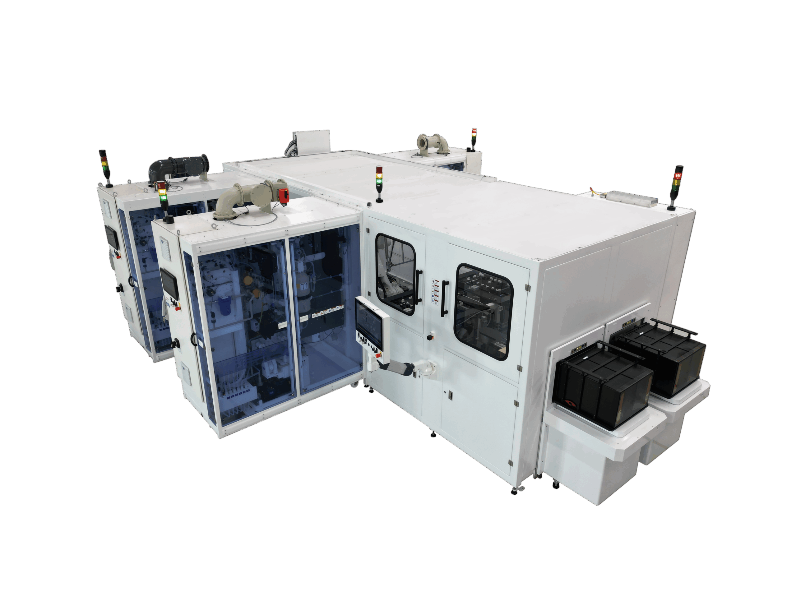
C+
Wet tools for developing, etching, stripping, cleaning and bond processes
P+
High end plater for thin seed layer copper applications
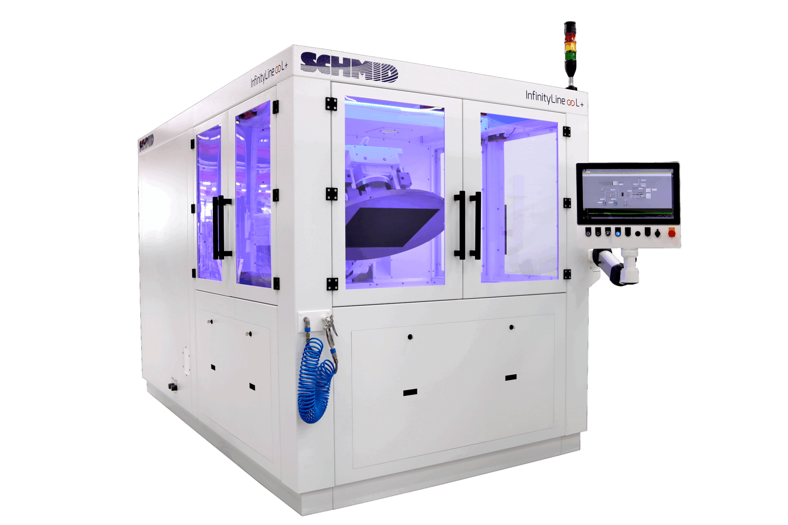
L+
Chemical mechanical polishing for full format panels

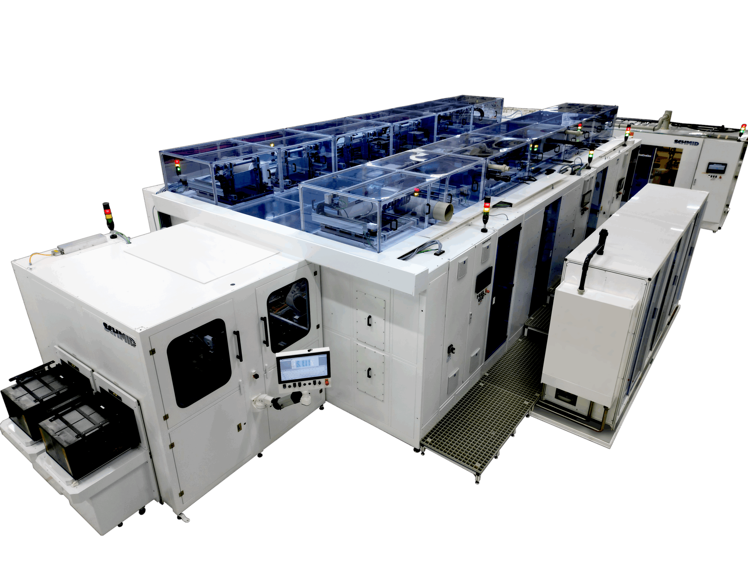
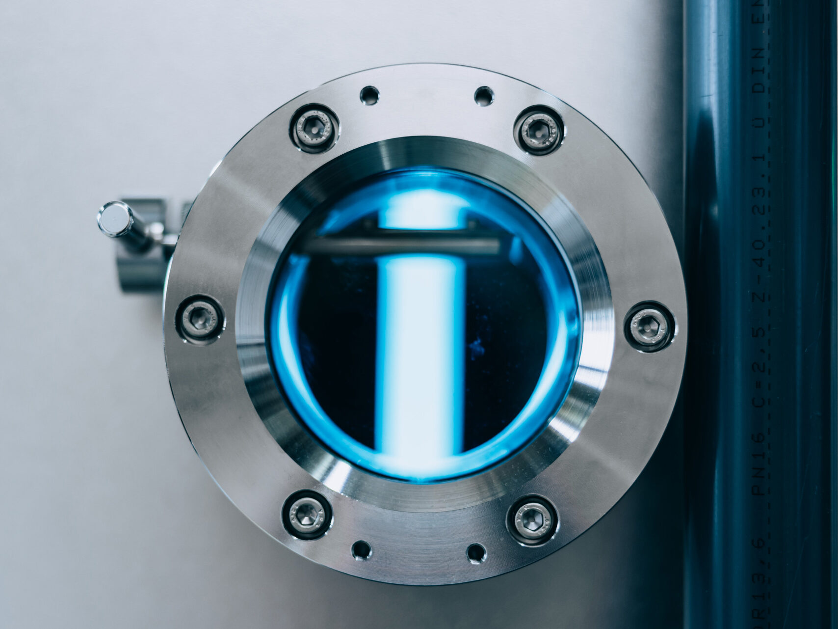
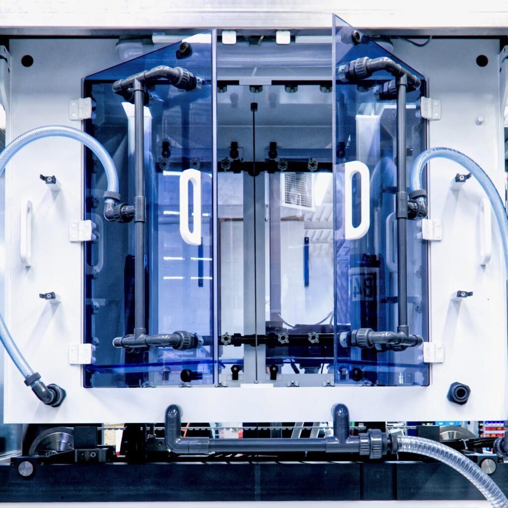
PlasmaLine
S line for deep etching of the base material and D line for desmearing, roughening the material and sputtering Ti and Cu. During all processes the panels are staying in a “clean” environment. All process area of the machines is classified in clean room ISO6. The transport from a machine to another machine is done per a FOUP system which maintains the panels in a clean and controlled environment. The panels are clamped on a frame with magnetic fingers or deposed on a tray which minimizes the contact with the active surface.

Details
Starting on a core or directly on a raw material a layer of ABF or other non-fiber material will be laminated. The board is processed on both sides in a line by a plasma sputtering process, in which a thin Cu layer is deposited. The patterning of drilling image will be done: resist lamination, exposure, development and Cu flash etching.
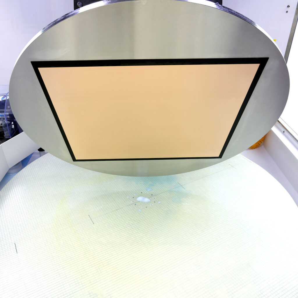
The panel will be transported to a cluster vertical static plasma etching system (ICP RIE). The system consists of 6 fully automated process modules. Inside the process module, 2 panels can proceed simultaneously. The panel is maintained on an ESC chuck cooled with He during the etching of the base material. The resist will be stripped during the etching process.
The next steps will be the patterning of the traces: resist lamination, exposure, development and Cu flash etching. The second process step with Plasma etching to finalize the etching of the holes and at the same time, etching the traces. A flash etching to remove the Cu from the surface will be proceeded.
The board will be double side processing in line through a Plasma Sputtering: first step will be a roughening and cleaning of the organic surface following a Ti or TiNx as adhesion layer and finally a Cu sputtering seed layer of minimum 800nm.
The next step will be to filling the trace and the microvias with the electro plating Cu. This step requires a high uniformity plating results for minimizing the time of the next process which is the CMP. We obtain this high uniformity with a single cell plating system with optimized multi directional flow system integrated, segmented anodes to control the copper distribution, sealed and water-cooled titanium contacts optimized for plating on thin seed layers.
Finally, the last steps will be the CMP process using the “Oscar” type of working principal. This process is a complex process that requires precise machine recipes along with good plating and tailored slurry.

Product Benefits
Greater thermal dissipation is required from the die to extend package life and ensure function
Embedded circuit trace pattern
Increase the Cu density
Planarity improvement
Deliver high density I/O
Controlled impedance to minimize signal loss
Change the interconnection geometry
Other equipment for electronics
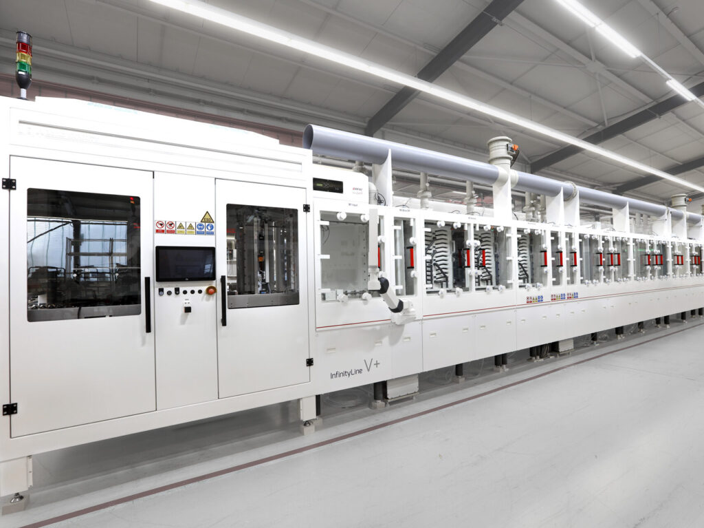
Vertical and Horizontal Wet Process
With our different lines InfinityLine H+ and V+, we offer horizontal and vertical wet processing to fulfill all demands of future-oriented technologies such as SAP and mSAP in serial production for the Advanced HDI and IC substrate markets.
Vacuum Metalization & Etch
Our inductively coupled plasma modules enable efficient besmear and surface treatment of low loss high frequency substrate materials, as well as deposition of dielectric layers.
Plating
Find out about our modular vertical touch free plating clusters. For different plating applications, adjustable shieldings, diaphragma, vertical or laminar parallel electrolyte flow are available.
Chemical Mechanical Polishing
The novel SCHMID CMP (Chemical Mechanical Polishing) line for large substrates stands as a solution for the decisive step for the next generation of multilayer PCBs and substrates. The SCHMID CMP offers a new universe for PCB designs in combination with the SCHMID embedded trace technology.
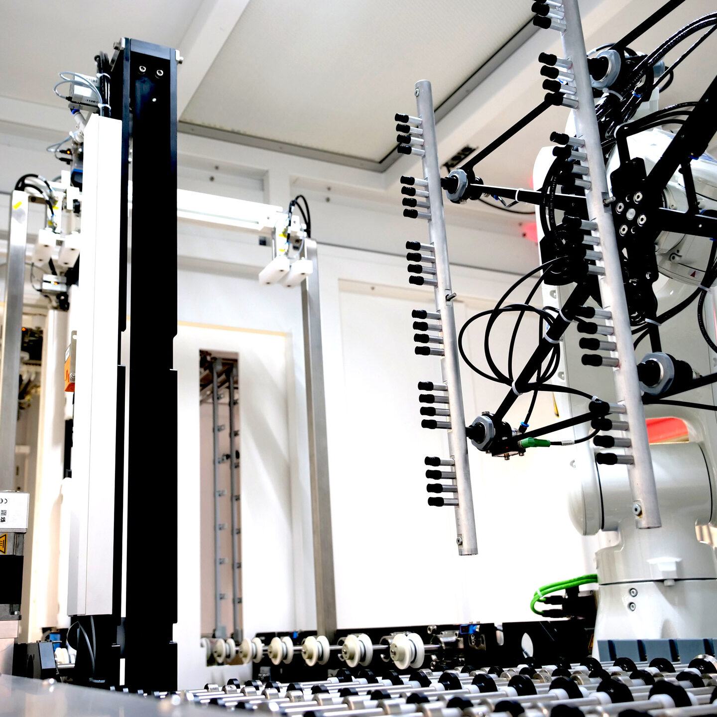
Automation
In addition to the wet processes, we are specialized in automation systems for the electronics market. We automate individual machines, to be integrated into innovative Smart Factories.