


PlasmaLine
Plasma etch and deposition for HDI+ PCB’s and IC substrates
PlasmaLine is a series of modular inline plasma systems for touch-free, simultaneous double-side processing of high end HDI+ PCBs and IC substrates. By combining etch and deposition process modules, the system can be configured for almost any application.
Inductively coupled plasma modules enable efficient desmear and surface treatment of low loss high frequency substrate materials, as well as deposition of dielectric layers. Magnetron sputter modules allow the deposition of adhesion and seed layers, which are increasingly used in semi-additive processing (SAP) and modified SAP (mSAP).
Details
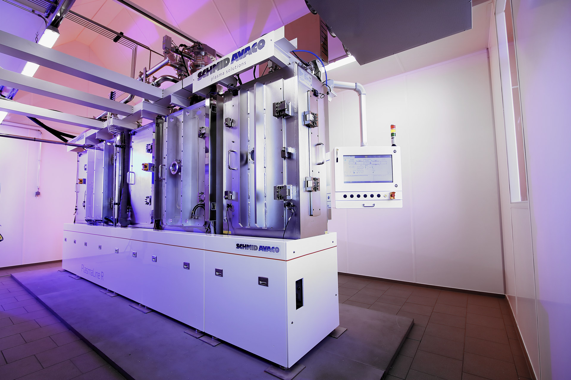
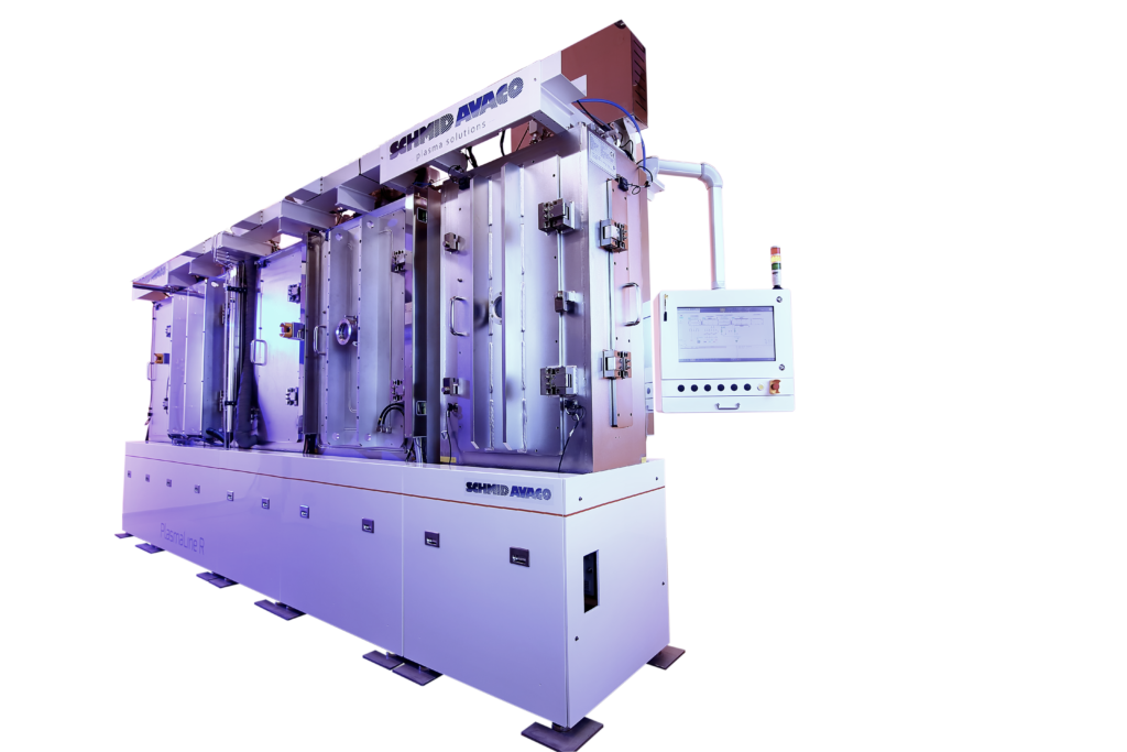
PlasmaLine is a multi-process tool for processing of HDI+ boards and substrates. The systems have a modular in-line design for dynamic, simultaneous double-side etching and deposition processing on rigid and flexible materials. The vertical orientation of the panel-in-frame and a magnetic drive provides touch-free transport and a particle-free environment.
Within the PlasmaLine there are load-lock modules, inductively coupled plasma modules (ICP), magnetron sputter physical vapor deposition modules (MS PVD), and radiation cooling modules. The ICP module can be used for dry etch, desmear, and surface treatment and for plasma enhanced chemical vapor deposition (PECVD) of dielectric layers. The PVD modules are composed of two pairs of planar magnetrons with double race tracks for simultaneous coating of both panel sides. The PVD process is part of the SAP process to deposit a copper (Cu) seed layer on dielectric materials before pattern plating.
The smallest configuration is the PlasmaLine R, which is intended for research and low volume production of next generation high frequency products. The Plasma-Line M is a fully automated production tool comprising plasma etch and sputter deposition modules for mass manufacturing of HDI+ boards and IC substrates. The low cost of ownership makes it a perfect solution for mSAP and SAP processing.
Technical data
Panel size and thickness:
- Panel size: 12“ x 18“ – 24“ x 24“
- Thickness: (10 – 1000) μm /extension possible
- Material: any material with Tg > 150ºC
Processing:
- ICP etch: desmear, descum, activation, etc.
- ICP PECVD: SiO2, SiOxNy, other dielectrics
- Sputter PVD: Cu, Ti, other films
Process specification:
- Panel transport: 0 – 5 m/min
- Temperature: max. 140ºC (controlled)
- Gas supply
- ICP: 6 channels
- PVD: 2 channels
- Dynamic etch rate*: up to 400 nm*m/min
- Dynamic Cu deposition rate**: up to 200 nm*m/min
- Dynamic Ti deposition rate**: up to 100 nm*m/min
- Uniformity: 5 %
* one module; ** one sputter head
Tact time (production tool)
- 15 sec per panel

Contact
We look forward to getting to know you!
Simply select your region and leave us a message.
EUROPE
CHINA
Tracy Xie
xie.tr@schmid-group.com
TAIWAN
Johnny Tseng
tseng.jo@schmid-group.com
KOREA
Jaho Kim
kim.jh@schmid-group.com
REST OF ASIA
AMERICA